! Under Construction, use at own risk !
Updated : Feb.17,1999
Updated PCB layout in work (maybe end of this week), fixes will be:
- insufficient space for one or two of the capacitors,
- illegible PCB components markings
- PCB size 'over-optimized' for specific box, change to more 'squarish'.
- clip sync output to TTL level - seems to take some more time to fit the extra parts on the board; as a quick fix, put a ZPD 4.7 (4.7 V Z-Diode) between SG and ground at the POWER switch (ring to SG) and a 1k resistor between the SG output from the BOT PCB and the SG pad of the power switch to clip SYNCOUT to 4.7V :
(BOT SG)--1k--(POWER SG)--|ZPD4.7--(GND)
Done Feb 16:
- extra page with all small pics for easier printing/download
( no pictures of the device yet, waiting for my photos getting developed - but the prototype works, honestly)
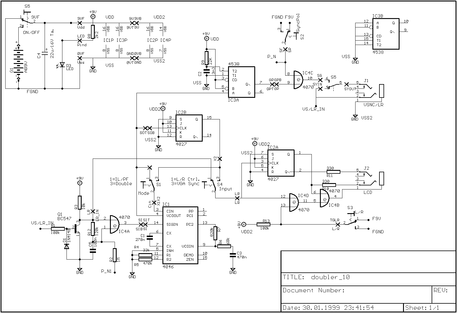
This controller is based mainly on the circuit by Thomas Schuhmann & Franz Krause. I added some improvements and simplifications (which I may have seen in other circuits, so credits go to all those nice people that contributed to the homebrew section at stereo3d.com ).
With some heavy redesign of the PCB, I made the whole stuff fit into a much smaller box.
All necessary parts together should cost not more than approx. 50 DM / 25 EUR / 30 US$.
The controller provides the following operating modes :
VGA pass-through for interlaced and page-flip stereo modes
VGA sync-doubler for top-bottom stereo mode
external L/R switch signal for connection to serial, parallel or 3-pin VESA mini-DIN port.
Additional features:
L/R toggle switch
Automatic adaptation of generated V-Sync polarity, may be forced to positive resp. negative.
Compact design (fits into 10cm x 6 cm hand-held box with 9V battery)
Improvements / changes w.r.t. the device by Thomas & Franz:
PLL circuit fine-tuned for less jitter - Thomas once told me that he just used an out-of-the-box circuit for frequency multiplication, which had a far too wide frequency range (~10 kHz) to be really stable at usual V-sync frequencies (~100 Hz). I restricted the range to approx. 25..300 Hz and get a rock-steady picture now.
Automatic adaptation of generated V-Sync polarity. The original circuit didn't care for the polarity (positive or negative pulses) of the V-sync signal, but always synchronize to the rising edge of the pulse. My circuit automagically converts the received V-sync signal to positive polarity, and the generated sync signal back to the received polarity, keeping the first edges of received and generated signal in sync regardless of polarity.
Combines 'the best of both worlds' w.r.t. shutter glasses driving: Like the original Cyberboy controller, I use a (spare from the sync-doubler) flip-flop to get half of the L/R switching frequency to toggle the polarity of the glasses (in contrast to the extra oscillator in the standard 4070-homebrew driver). Unlike the Cyberboy, however, I don't use an additional negative supply voltage, but instead drive the common line for both LCDs reversed to the currently active LCD (as in the standard 4070-homebrew driver).
The controller is designed for 'stupid' LCD shutter glasses with a 3.5 mm stereo connector like the Woobo Cyberboy, where the three wires are :
Left/Right LCD panel (tip/ring, or vice versa?), Common (base)
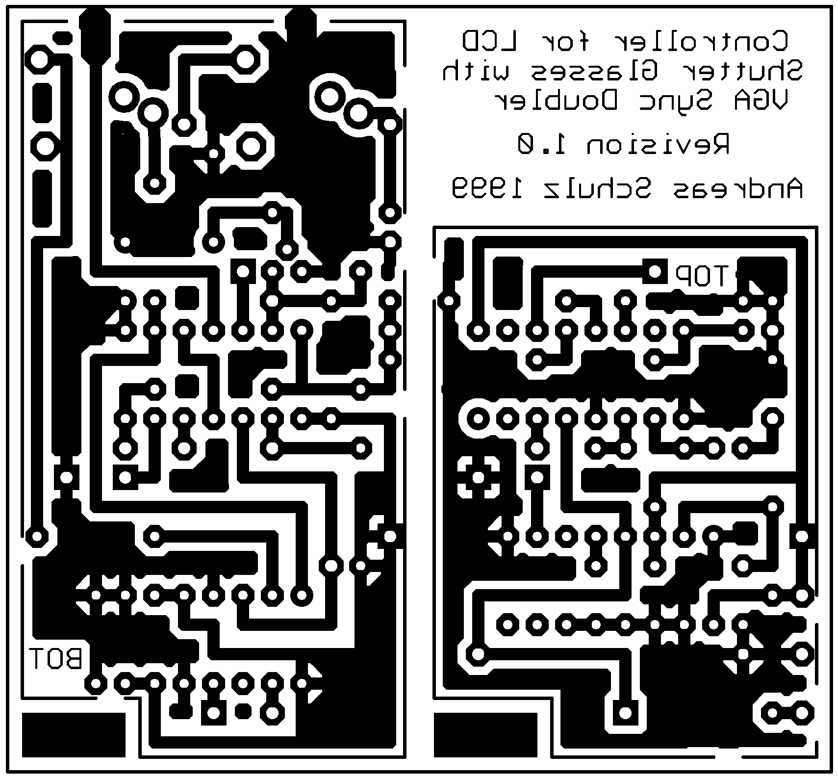
If you already own (or are willing to download the 4 MB free light/evaluation version of) EAGLE CAD, you can download a ZIP archive with the EAGLE sources for the circuit schematics and PCB layout
Otherwise, files are available for download for
Since I don't know your printer, you will have to use a picture editor like Picture Publisher, MS Photopaint etc. to convert the PCB layout to your printer's resolution. I've had cases where the editor assumed a resolution of 96 dpi, which would give a ridiculously large image.
You can find a very easy way to put the layout onto the PCB (besides the traditional photographic method) for etching at this site :
If you have (access to) a laser printer, just print the layout as it is (i.e. mirrored) and iron the laser toner onto the (clean) copper side of the PCB. Then soak the paper with warm water until you can gently peel and rub it off until (almost) only the laser toner remains on the PCB.
For best results, print at least twice on the same page to get an extra thick toner layer (although it will be hard to get the prints exactly in the same place).
Normal printer paper (kind of) works, but may leave some paper fibres. I also tried coated Hi-Res inkjet paper, which seems to have finer fibres, but only does a little better job.
Instead of a laser printer, you can get the same result using a photocopier with an inkjet printout (but be aware that some copiers don't scale properly).
If you are used to make PCBs by photo-transfer, just print the board layout in original size on a sheet of overhead projection film (as recommended for your printer) and expose as usual (printed side to the PCB, so you can read the text).
Having etched the PCB, cut out the two parts along the inner thin lines. I had to cut out the lower left corners to get around the screw that holds my case together - that's why the black rectangles are there.
Drilling : 1.5mm ? for 3.5mm jack pins (4 holes, base pin bent around PCB edge), 0.8mm ? for all others. Enlarge holes for IC socket pins to 1.5mm on the components side (see below); put board on a metal plate to avoid drilling through the copper film.
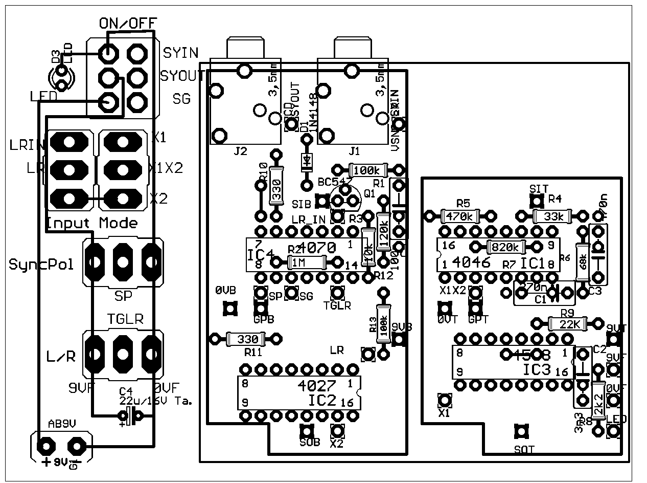
The circuit is designed to consist of two PCBs, with the smaller one mounted on top of the other, connected by 5 vertical wires, five external switches and an external LED.
Since space is very limited, you should either
(if you're very brave) solder the chips directly to the PCB. In this case, some resistors and wire connections that are underneath the ICs must be soldered to the copper side of the PCB. - or :
use very flat sockets, like the socket shown in this picture . To save another mm in height, widen the pinholes on the PCB's components side to 1.5 mm to accomodate the wider parts of the socket's pins - as shown in this drawing.
Crucial parts are also the 3.5mm stereo jacks, which must look like this to fit into the PCB (Hirschmann part No. PG203J). Note that the pins for the base contact have to be bent around the edge of the PCB to be soldered to their pads. In case you cannot find such jacks, you can also use ordinary 3.5mm stereo jacks for front-panel mounting and wire them to the PCB. In this case, you should cut the lower left edge of the TOP PCB only to have a place for drilling a hole in the BOT PCB for mounting the PCB stack to the box.
Holes for resistors are all 10mm apart, so there should be no problem for 1/4 W resistors. For capacitors, default distance is 7.5 mm, but try to get 10mm raster types for the 270n and 470n caps, since the 7.5mm types will be too wide and high. Some extra holes are available to allow 5, 7.5 or 10 mm raster sizes when other sizes are not available.
With all electronic parts soldered in place, now cut all pins and wire ends standing out on the copper sides of the PCBs as short as possible.
Next, you need five pieces of wire, approx. 2 cm in length (wire ends cut off the resistors should do). Solder them to the five square pads of the smaller PCB, standing out in full length from the copper side.
Before soldering the two PCBs together, you must solder 13 suffiently long thin isolated wires to the wirepads on the PCBs for connection to the switches, battery and LED (they will not be accessible any more afterwards). Remember which wire goes where, it may be hard to determine once the boards are joined.
Then you may join the two boards, putting the smaller board on top of the larger and carefully threading the vertical wires of the top board through the corresponding holes in the bottom board (also with square pads). Put them together as close as possible, then solder the wires to the bottom board and cut off any extra wire length from the bottom board's copper side. As soon as I get my pictures developed, you will find a picture of the stack here (not yet, sorry).
Next (if you haven't got one already), get a box that is large enough for the PCB stack, a 9V battery and the switches. Drill holes for the jacks on the PCB, the switches and the power LED and mount all parts in place. Wire and solder the switches, LED and Tantal Cap as shown in the componets drawing. Finally, solder the wires to the PCB stack to the corresponding terminals on the switches and LED.
If you now plug in your shutter glasses and power the device, the LED should light.
In page-flip or sync doubling mode, the glasses should flicker with a frequency of 20-30 Hz.
In direct-L/R-control mode, one of the LCDs should be dark, and you can change sides using the L/R toggle switch.
If you prefer to use an external source of 9-12V DC (from the PC or a wall plug adaptor), you may leave out the battery and add a corresponding jack.
The SYNC Polarity switch (S2) is not really needed, the automatic adaptation should do quite well (and you can save the extra money for a three-way switch, which usually costs extra).
If you only need shutter control from the VGA connector (page-flip and sync-doubling), you can also do without the 'Input' switch (S4) and connect the wire to the 'LR' pad directly to the 'X2' signal on the mode switch (S1).
The output frequency of the 4046 may vary considerably for the same external circuit between different chips. The frequency of the V-Sync output with open input should be around 25Hz +/- a few Hz. If not, the capacitor C1 (270n) should be rescaled accordingly.
I added the order numbers and prices of Conrad Electronics, Germany to the parts list since their catalogue is available online on the WWW (though usually quite busy), at least as a reference.
I found that there are also tiny 12V - batteries (AAA...ish size) which would be perfect for even better shading, if you can find a corresponding battery holder. But better wait with this until I add the clipping to TTL level for the V-sync output.
Direct L/R control from serial, parallel or VESA 3pin DIN port
You have to build an adaptor cable for the corresponding port (serial for the cyberboy, parallel for others, DIN-3 anyone?) according to the pinouts in this drawing In case of doubt, check your glasses' manual and Christoph's site.
Plug an adaptor cable for the desired port as (described above) into the L/R-VSYNC input jack of my controller. If you want to leave the VGA dongle in place, you need another 3.5 mm stereo jack with the ring and tip connectors soldered together.
Into this you can plug the dongle's plug to connect the computer's V-sync out to the monitor's V-sync in.
Set the input switch on the controller to 'L/R'.
You need a driver like LCDBios and corresponding software to support switching of the LCD glasses via ports.
Control by VGA vertical Sync
You have to build a VGA dongle according to the pinouts in this drawing, routing the vertical sync signal through my controller and all other signals connected straight through.
Plug the 3.5 mm stereo plug of the VGA dongle into the L/R-VSYNC input jack of my controller.
Set the input switch on the controller to 'VSYNC' and the mode switch to 'x1' resp. 'page-flip/interlace'.
You need either :
- software that does page-flipping, i.e. automatically toggles left and right picture every video (VSync-) frame, or
- a VGA board that supports interlaced video modes, i.e. displays even and odd pixel lines alternating in every other video (VSync-) frame and software (or stereo pictures) with left and right-eye images interleaved. This mode is also Windows desktop -compatible, at least for viewing stereo pics.
Sync-Doubling
Put the plug from the VGA dongle into the L/R-VSYNC input jack of my controller.
Set the input switch on the controller to 'VSYNC' and the mode switch to 'x2' resp. 'sync-double'.
You need software that puts the left and right-eye pictures in the top and bottom half of the screen, separated by some black lines for vertical re-tracing, and a non-interlaced VGA video mode. The controller will insert an extra V-sync pulse in the middle of the screen, causing the monitor to restart displaying from the top.
I have no 3D-software with native support for this mode, but a first test with a stereo picture pair, glued together with Picture Publisher and displayed full-screen at 800x600 resolution worked.
Toggle L/R
When in stereo mode the 3D-perspective 'doesn't seem right', most likely you see the left and right pictures reversed. In fact, since the controller does not have any L/R information when tapping the VGA vertical sync signal, you only have a 50-50 chance that the relation between picture and LCD is correct. For those glasses that don't have a L/R toggle switch built in (the Cyberboy has), the controller has its own L/R toggle.
Force Sync Polarity
Normally, you should leave the sync polarity switch in middle (neutral) position. Thus, the sync signal generated cy the controller will have the same polarity as the signal received from the VGA controller.
In sync doubling mode, you may try to toggle the sync polarity by setting the switch left or right (depending on the input signal, only one position will have an effect).
Switch from VGA-sync control to direct (serial/parallel/VESA 3pin DIN port) L/R control by just plugging the adaptor into a third jack.
Add line-blanking mode like in the new CyberJoy controller. The controlling circuit should need just an additional flip-flop and an xnor-gate for the H-sync, but the blanking switches to pull the RGB signal levels to black every second line look critical (bandwidth, impedance matching etc.). The MAXIM MAX4019 (triple video buffer with output disable) and MAX499 (RGB video switch) look promising, but seem to be hard to find.
(far future) Put the whole logic into a PIC program for an even smaller device that would allow automagical detection of operating mode and push-button control. First guess is that even an 8-pin (6 I/O lines) controller should do already, but I guess I should prefer a good ol' 16C84. Found a good PIC site at David Tait's
The circuit was designed with the Light version of EAGLE CAD from CADSoft.